
allisonaparrish@friend.camp
Sep 21, 2026, 8:18 PMi made this simplified diagram of the Game Boy's internals (DMG) for the talk I gave at the NYC Permacomputing meetup a few weeks ago and thought I'd also share it here
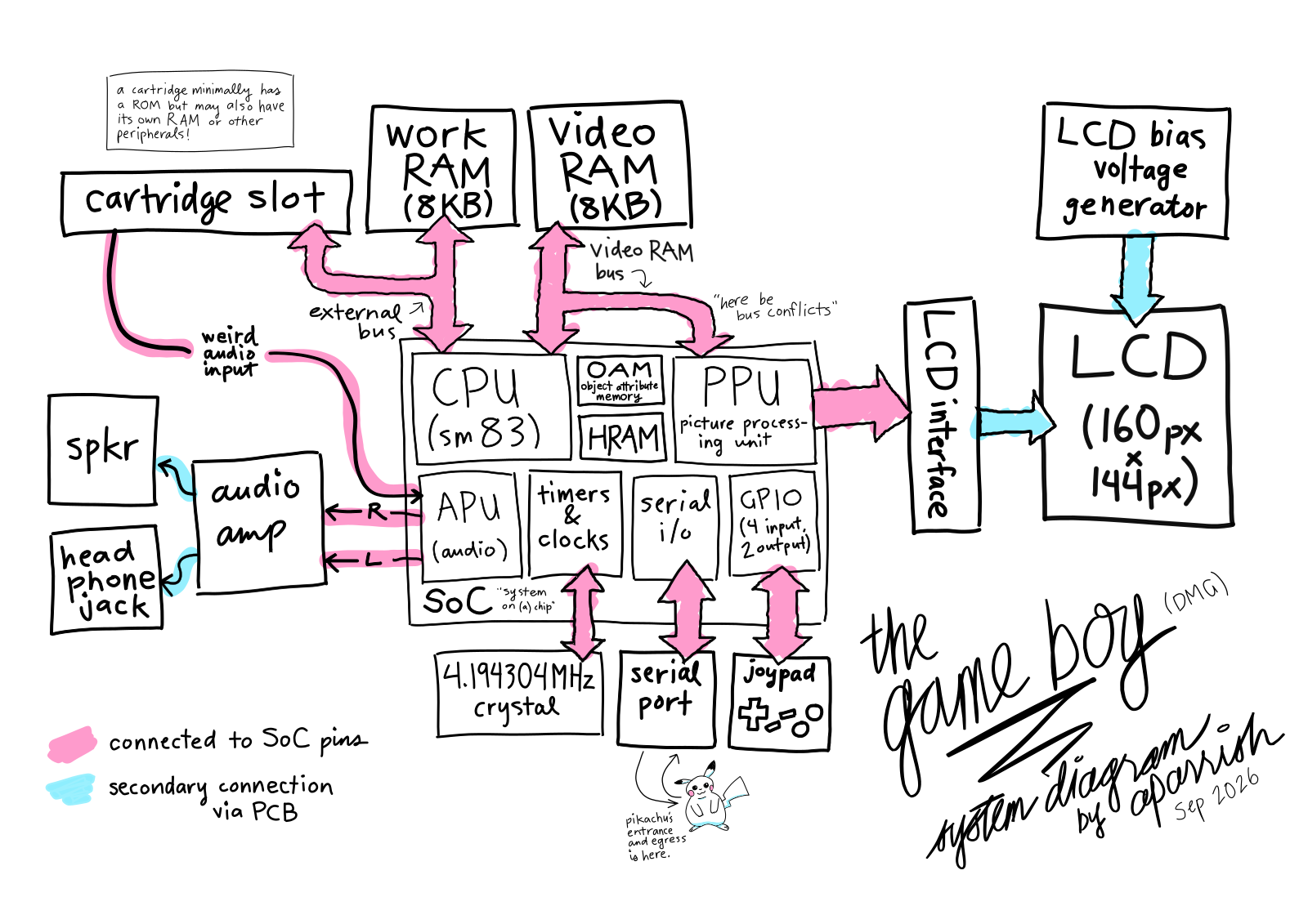
i made this simplified diagram of the Game Boy's internals (DMG) for the talk I gave at the NYC Permacomputing meetup a few weeks ago and thought I'd also share it here
(i specify DMG because each of the subsequent Game Boy models has different arrangements of components! the Pocket has largely the same pinout as the DMG but the VRAM was moved into the SoC. the Color SoC has internal VRAM, and has separate external buses for the cartridge slot and for the work RAM, presumably because the Color's work RAM is 3.3v but cartridges still need 5v. the "revision E" of the Color moved the work RAM into the SoC as well)